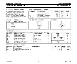
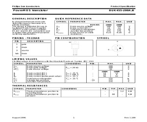
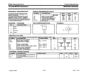
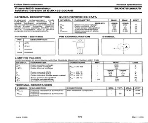
t Tj RDS(ON) BUK455 Drain-source voltage Drain current (DC) Total power dissipation Junction temperature Drain-source on-state resistance -200A 200 14 125 175 0.23 -200B 200 13 125 175 0.28 V A W C PIN CONFIGURATION DESCRIPTION 1 gate 2 drain 3 source tab BUK455-200A/B SYMBOL d tab g drain s 1 23 LIMITING VALUES Limiting values in accordance with the Absolute Maximum System (IEC 134) SYMBOL PARAMETER CONDITIONS MIN. MAX. UNIT VDS VDGR VGS Drain-source voltage Drain-gate voltage Gate-source voltage RGS = 20 k - - 200 200 30 V V V ID ID IDM Drain current (DC) Drain current (DC) Drain current (pulse peak value) Tmb = 25 C Tmb = 100 C Tmb = 25 C - Ptot Tstg Tj Total power dissipation Storage temperature Junction Temperature Tmb = 25 C - - 55 - -200A 14 10 56 -200B 13 9 52 A A A 125 175 175 W C C THERMAL RESISTANCES SYMBOL PARAMETER Rth j-mb Thermal resistance junction to mounting base Thermal resistance junction to ambient Rth j-a April 1993 CONDITIONS 1 MIN. TYP. MAX. UNIT - - 1.2 K/W - 60 - K/W Rev
 7 Pages, 43 KB, Original
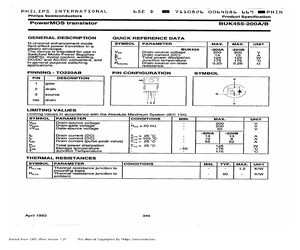
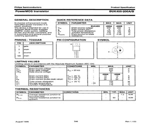
BUK455-200A/B a GENERAL DESCRIPTION QUICK REFERENCE DATA N-channel enhancement mode SYMBOL | PARAMETER MAX. | MAX. | UNIT field-effect power transistor in a plastic envelope. BUK455 -200A | -200B The device is intended for use in Vos Drain-source voltage 200 200 Vv Switched Mode Power Supplies Ip Drain current (DC) 14 13 A (SMPS), motor control, welding, Pia Total power dissipation 125 125 W DC/DC and AC/DC converters, and T Junction temperature 175 175 Cc in general purpose switching Fosom Drain-source on-state 0.23 0.28 Q applications. resistance PINNING - TO220AB PIN CONFIGURATION SYMBOL PIN DESCRIPTION | d tab > CG 1 Igate =~ , | | hh 2 {drain _! i | ie x ; tp 3 |source 1 " 9 SHY fy ; tab |drain - | | 123 s LIMITING VALUES Limiting values in accordance with the Absolute Maximum System (IEC 134) SYMBOL |PARAMETER CONDITIONS MIN. MAX. UNIT Vos Drain-source voltage - - 200 Vv Vocr Drain-gate voltage Ras = 20 kQ - 200 Vv Ves Gate-source voltage - - 30 Vv -200A -200B lo Drain current (DC Tr = 25C
 5 Pages, 242 KB, Scan
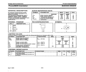
BUK455-200A/B GENERAL DESCRIPTION QUICK REFERENCE DATA N-channel enhancement mode SYMBOL | PARAMETER MAX. MAX. UNIT field-effect power transistor in a plastic envelope. BUK455 -200A | -200B The device is intended for use in Vos Drain-source voltage 200 200 Vv Switched Mode Power Supplies lb Drain current (DC) 14 13 A (SMPS), motor control, welding, Prot Total power dissipation 125 125 Ww DC/DC and AC/DC converters, and T, Junction temperature 175 175 C in automotive and general purpose Rosiony Drain-source on-state 0.23 0.28 Q switching applications. resistance; PINNING - TO220AB PIN CONFIGURATION SYMBOL PIN DESCRIPTION or () d 1 |gate _ 7 : It a 2 {drain i i yes iI 3 |source \ i Foe! fe tab [drain | | 123 $s LIMITING VALUES Limiting values in accordance with the Absolute Maximum System (IEC 134) SYMBOL |PARAMETER CONDITIONS MIN. MAX. UNIT Vos Drain-source voltage - - 200 Vv Vocr Drain-gate voltage Reg = 20 kQ - 200 Vv Ves Gate-source voltage - - 30 Vv -200A -200B lp Drain current (DC) Tab = 25C
 5 Pages, 225 KB, Scan
 Tj RDS(ON) BUK455 Drain-source voltage Drain current (DC) Total power dissipation Junction temperature Drain-source on-state resistance; -200A 200 14 125 175 0.23 -200B 200 13 125 175 0.28 V A W C PIN CONFIGURATION DESCRIPTION 1 gate 2 drain 3 source tab BUK455-200A/B SYMBOL d tab g drain s 1 23 LIMITING VALUES Limiting values in accordance with the Absolute Maximum System (IEC 134) SYMBOL PARAMETER CONDITIONS MIN. MAX. UNIT VDS VDGR VGS Drain-source voltage Drain-gate voltage Gate-source voltage RGS = 20 k - - 200 200 30 V V V ID ID IDM Drain current (DC) Drain current (DC) Drain current (pulse peak value) Tmb = 25 C Tmb = 100 C Tmb = 25 C - Ptot Tstg Tj Total power dissipation Storage temperature Junction Temperature Tmb = 25 C - - 55 - -200A 14 10 56 -200B 13 9 52 A A A 125 175 175 W C C THERMAL RESISTANCES SYMBOL PARAMETER Rth j-mb Thermal resistance junction to mounting base Thermal resistance junction to ambient Rth j-a August 1996 CONDITIONS 1 MIN. TYP. MAX. UNIT - - 1.2 K/W - 60 - K/W Re
 7 Pages, 53 KB, Original
BUK455-200A/B ee ee ee er ee ee ee eee GENERAL DESCRIPTION QUICK REFERENCE DATA N-channel enhancement mode SYMBOL | PARAMETER MAX. MAX. UNIT field-effect power transistor in a - plastic envelope. BUK455 -200A | -200B The device is intended for use in Vos Drain-source voltage 200 200 Vv Switched Mode Power Supplies | Drain current (DC) 14 13 A (SMPS), motor control, welding, P Total power dissipation 125 1. 125 Ww DC/DC and AC/DC converters, and T Junction temperature 175 175 Cc in automotive and general purpose Psion) Drain-source on-state 0.23 0.28 Q switching applications. resistance; PINNING - TO220A8 PIN CONFIGURATION SYMBOL PIN DESCRIPTION mp O 4 1 |gate 7 2 {drain | 3 |source ) | 9 tab [drain I 123 LIMITING VALUES Limiting values in accordance with the Absolute Maximum System (IEC 134) SYMBOL | PARAMETER CONDITIONS MIN. MAX. UNIT Vos Drain-source voltage - - 200 Vv Voar Drain-gate voltage Reg = 20 kQ 200 Vv Ves Gate-source voltage - - 30 Vv -200A -200B lb Drain current (BE Tre = 25C - 14 13
 5 Pages, 285 KB, Scan
BUK455-200A/B Dn GENERAL DESCRIPTION QUICK REFERENCE DATA N-channel enhancement mode SYMBOL | PARAMETER MAX. MAX. UNIT field-effect power transistor in a plastic envelope. BUK455 -200A | -200B The device is intended for use in Vos Drain-source voltage 200 200 Vv Switched Mode Power Supplies Ip Drain current (DC) 14 13 A (SMPS), motor control, welding, Prot Total power dissipation 125 125 WwW DC/DC and AC/DC converters, and i Junction temperature 175 175 C in automotive and general purpose Rosion Drain-source on-state 0.23 0.28 Q switching applications. resistance; PINNING - TO220AB PIN CONFIGURATION SYMBOL PIN DESCRIPTION wh Ce J d 1 gate 2 drain f | 3 |source ) 9 N / tab |drain i 123 s LIMITING VALUES Limiting values in accordance with the Absolute Maximum System (IEC 134) SYMBOL |PARAMETER CONDITIONS MIN. MAX. UNIT Vos Drain-source voltage - - 200 Vv Voer Drain-gate voltage Res = 20 kQ - 200 Vv Ves Gate-source voltage - - 30 Vv -200A -200B lp Drain current (Be Trp = 25 C - 14 13 A Ip Drain curr
 5 Pages, 175 KB, Scan
BUK455-200A/B GENERAL DESCRIPTION QUICK REFERENCE DATA N-channel enhancement mode SYMBOL | PARAMETER MAX. | MAX. UNIT field-effect power transistor in a plastic envelope. BUK455 -200A | -200B The device is intended for use in Vos Drain-source voltage 200 200 Vv Switched Mode Power Supplies Ip Drain current (DC) 14 13 A (SMPS), motor control, welding, Poot Total power dissipation 125 125 WwW DC/DC and AC/DC converters, and T Junction temperature 176 175 Cc in general purpose switching Rosiom Drain-source on-state 0.23 0.28 2 applications. resistance PINNING - TO220AB PIN CONFIGURATION SYMBOL PIN DESCRIPTION re d 1 |gate aN ! 1 2 {drain K) 3 |source } iH g tab [drain | | | 123 s LIMITING VALUES Limiting values in accordance with the Absolute Maximum System (IEC 134) SYMBOL |PARAMETER CONDITIONS MIN. MAX. UNIT Vos Drain-source voltage - - 200 Vv Vocr Drain-gate voltage Res = 20 kQ - 200 Vv Ves Gate-source voltage - - 30 Vv -200A -200B lo Drain current be} Tb = 25 C - 14 13 A lp Drain current (DC Tp
 5 Pages, 189 KB, Scan
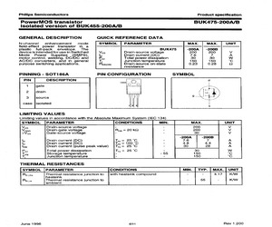
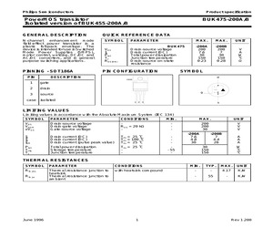
BUK455-200A/B GENERAL DESCRIPTION QUICK REFERENCE DATA N-channel enhancement mode SYMBOL | PARAMETER MAX. MAX. UNIT field-effect power transistor in a plastic full-pack envelope. The BUK475 -200A | -200B device is intended for use in Switched Vos Drain-source voltage 200 200 Vv Mode Power Supplies (SMPS), lp Drain current (DC) 7.6 7 A motor control, welding, DC/DC and Prot Total power dissipation 30 30 Ww AC/DC converters, and in general ; Junction temperature 150 150 Cc purpose switching applications. Rosion) Drain-source on-state 0.23 0.28 Q resistance PINNING - SOT186A PIN CONFIGURATION SYMBOL PIN DESCRIPTION Oo d case Soa 1 ate a Ary 2 |drain | _s 3 source \ $ NN J) case |isolated | Vj s LIMITING VALUES Limiting values in accordance with the Absolute Maximum System (IEC 134) SYMBOL |PARAMETER CONDITIONS MIN. MAX. UNIT Vos Drain-source voltage : - 200 Vv Voer Drain-gate voltage Rags = 20 kQ - 200 Vv +Ves Gate-source voltage - - 30 Vv -200A -200B Ip Drain current (DC Ths = 25 C - 7.6 7 A Ib Dra
 5 Pages, 290 KB, Scan
BUK455-200A/B eee ee ee ee ee ee eee GENERAL DESCRIPTION QUICK REFERENCE DATA N-channel enhancement mode SYMBOL | PARAMETER MAX. MAX. UNIT field-effect power transistor in a plastic full-pack envelope. The BUK475 -200A | -200B device is intended for use in Switched Vos Drain-source voltage 200 200 Vv Mode Power Supplies (SMPS), Ip Drain current (DC) 786 7 A motor control, welding, DC/DC and Prot Total power dissipation 30 30 Ww AC/DC converters, and in general T Junction temperature 150 150 Cc purpose switching applications. Rosiony Drain-source on-state 0.23 0.28 Q resistance PINNING - SOT186A PIN CONFIGURATION SYMBOL PIN DESCRIPTION Oo d case O O 1 gate ok / 2 {drain we \ W oT) 3 |source \ WA case |isolated | Wye s LIMITING VALUES Limiting values in accordance with the Absolute Maximum System (IEC 134) SYMBOL |PARAMETER CONDITIONS MIN. MAX. UNIT Vpbs Drain-source voltage - - 200 Vv Vocr Drain-gate voltage Regs = 20 kQ - 200 Vv +Veg Gate-source voitage - - 30 Vv -200A -200B lo Drain current (BC
 5 Pages, 183 KB, Scan
BUK455-200A/B Cerner rere ere ee er eee eee GENERAL DESCRIPTION QUICK REFERENCE DATA N-channel enhancement mode SYMBOL | PARAMETER MAX. | MAX. UNIT field-effect power transistor in a plastic full-pack envelope. The BUK475 -200A | -200B device is intended for use in Switched Vos Drain-source voltage 200 200 Vv Mode Power Supplies (SMPS), lp Drain current (DC) 7.6 7 A motor control, weiding, DC/DC and Prot Total power dissipation 30 30 Ww AC/DC converters, and in general T, Junction temperature 150 150 C purpose switching applications. Rosion) Drain-source on-state 0.23 0.28 Q resistance PINNING - SOT186A PIN CONFIGURATION SYMBOL PIN DESCRIPTION d | 1 [gate g a \ 2 |drain 4 x 3 |source 9 TN tr case |isolated $s LIMITING VALUES Limiting values in accordance with the Absolute Maximum System (IEC 134) SYMBOL |PARAMETER CONDITIONS MIN. MAX. UNIT Vos Drain-source voltage - : 200 Vv Vogr Drain-gate voltage Reg = 20 kQ - 200 Vv Veg Gate-source voltage - - 30 Vv -200A -200B Ip Drain current Oy Ths = 25C -
 5 Pages, 245 KB, Scan
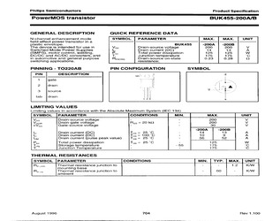
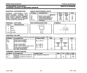
BUK455-200A/B GENERAL DESCRIPTION N-channel enhancement mode field-effect power transistor in a plastic full-pack envelope. The device is intended for use in Switched Mode Power Supplies (SMPS), motor control, welding, DC/DC and AC/DC converters, and in general purpose switching applications. PINNING - SOT186A PIN BUK475-200A/B QUICK REFERENCE DATA SYMBOL PARAMETER MAX. MAX. UNIT VDS ID Ptot Tj RDS(ON) BUK475 Drain-source voltage Drain current (DC) Total power dissipation Junction temperature Drain-source on-state resistance -200A 200 7.6 30 150 0.23 -200B 200 7 30 150 0.28 V A W C PIN CONFIGURATION SYMBOL DESCRIPTION d case 1 gate 2 drain 3 source g case isolated 1 2 3 s LIMITING VALUES Limiting values in accordance with the Absolute Maximum System (IEC 134) SYMBOL PARAMETER CONDITIONS MIN. MAX. UNIT VDS VDGR VGS Drain-source voltage Drain-gate voltage Gate-source voltage RGS = 20 k - - 200 200 30 V V V ID ID IDM Drain current (DC) Drain current (DC) Drain current (pulse peak value) Ths = 25 C T
 7 Pages, 56 KB, Original


